

For a decade, gallium nitride was the answer to a question most power engineers were not yet asking. That changed. Low-voltage GaN — the enhancement-mode discrete FET segment around 30 V to 200 V — moved from sampling quantities to a genuine design option with multiple qualified vendors, reference designs, and evaluation boards. For OEM and EMS teams this is the sweet spot: high enough switching frequency to shrink magnetics and raise efficiency, low enough voltage that gate drive, layout discipline, and sourcing stay tractable. This guide covers where low-voltage GaN actually wins, the five parameters that decide the GaN-versus-silicon question, and how to qualify GaN parts for a production build.
Why Low-Voltage GaN Reached the Mainstream
Two things moved low-voltage GaN from promising to practical. First, supply: what was a single-source eGaN portfolio became a multi-vendor market, with the major power semiconductor groups licensing technology and building internal wafer capability. Second-source availability is not a nice-to-have in production — it is the difference between a component you can schedule and a component you cannot. Second, application pull: the AI power-architecture shift toward 48 V intermediate buses, the continued spread of USB-PD high-power charging, and the push to shrink industrial power modules all reward exactly what GaN delivers — high dv/dt, low switching loss, and small magnetic components. Buyers who want to move on this should know which GaN and power semiconductor vendors are in production before committing a design.
The segment’s appeal is specific, and worth stating plainly: it is a low-voltage story. High-voltage GaN (650 V and above) is a different engineering problem with different risk profiles, and the supply picture is different again. If your rail is 48 V or 100 V, low-voltage enhancement-mode GaN is the relevant conversation.
The Five Parameters That Decide GaN Versus Silicon
1. Threshold Voltage and Gate Drive Complexity
Low-voltage eGaN devices are typically enhancement-mode with a threshold around 2 V, which means they drive from a standard low-side gate driver without the negative bias that depletion-mode or p-GaN devices require. That is a real engineering advantage: no negative rail, no special driver, fewer BOM parts. The tradeoff is gate drive speed. Because the device has essentially no reverse-conduction behavior and a very low body diode drop, switching transients are fast enough that a marginally-slow driver can increase switching loss substantially. Match the driver current to the device’s total gate charge, and check the layout before you trust a breadboard result.
2. RDS(on) at the Temperature That Matters
Silicon MOSFET datasheets quote RDS(on) at 25 °C. GaN datasheets typically quote it at 150 °C, or they tell you to derate. This is not a like-for-like comparison, and the gap widens with junction temperature. For any design running a hot converter — a laptop charger, a server power module, a compact industrial supply — the honest comparison is RDS(on) at your actual operating junction temperature. GaN wins comfortably below roughly 100 V bus at moderate-to-high current; the crossover is bus-voltage and thermal-design dependent, so compute it rather than assume it.
3. Switching Transition and dv/dt
This is the parameter that makes GaN interesting and also the one that punishes sloppy layout. A low-voltage enhancement-mode FET can switch transitions in nanoseconds with tens of volts per nanosecond. That is a feature in the converter, and a hazard on the board: high dv/dt couples into adjacent traces through parasitic capacitance, and the fast dI/dt in the commutation loop radiates. Two consequences follow. Keep the switching loop as small as possible, and treat the layout as part of the device, not as a downstream formality. Layout inductance that would be a minor inefficiency on a silicon design can dominate losses on a GaN design.
4. Common-Source Inductance and Gate Loop
The combination of high dv/dt and a high dI/dt makes the common-source inductance between package and die the dominant parasitic. Use the manufacturer’s recommended land pattern, place the gate loop resistor and driver close to the device, and if the part is offered in a specific high-frequency package, do not substitute a generic package for cost reasons. This is the most common field failure pattern in GaN designs, and it presents as “the device is fine on the bench but unreliable in the product.”
5. Part Number Stability and Lifecycle Commitment
A GaN design that ships for three years needs a part that will be available for three years, ideally with a pin-compatible second source. This is where the multi-vendor shift actually matters commercially, and it is a line item worth confirming with the manufacturer before you commit a design: is the device in production, is it the lead part or a sampling option, and does a pin-compatible alternative exist? Mature low-voltage eGaN portfolios are in a much better place on this question than they were three years ago, but it still needs asking.
Where Low-Voltage GaN Wins — and Where Silicon Does Not
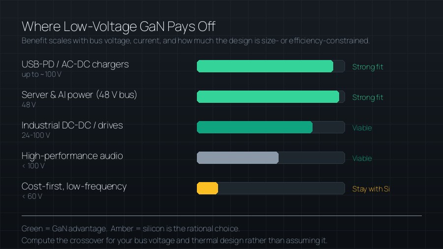
| Application | Bus Voltage | Why GaN Helps | Silicon Still Sufficient? |
|---|---|---|---|
| USB-PD / AC-DC laptop and tablet chargers | Up to ~100 V | Higher switching frequency shrinks transformer and magnetics; enables smaller, lighter designs | Only for cost-first, size-tolerant designs |
| Server and AI power conversion (48 V intermediate bus) | 48 V typical | High current at moderate bus; efficiency at high frequency; board area reduction | Rarely — efficiency targets push GaN |
| Industrial DC-DC and motor drive stages | 24–100 V | Lower switching and conduction loss in compact modules | At low current, silicon is cost-competitive |
| Audiophile and high-performance audio amplifiers | Low, <100 V | Class-D efficiency at high bandwidth | For entry-level audio, silicon is fine |
| Low-power, low-frequency, cost-first designs | <60 V | Minimal benefit; GaN premium not recovered | Yes — stay with silicon |
Checklist for Sourcing and Qualifying GaN Parts
- Confirm the rail. Low-voltage eGaN is a 30–200 V conversation. If your bus is 400 V or higher, you are looking at high-voltage GaN or silicon superjunction, a different sourcing problem.
- Ask for production status and lifecycle. Production part or sample? Any planned EOL? Is a pin-compatible second source available?
- Verify the package and land pattern. Do not substitute a generic package for a manufacturer-recommended high-frequency layout.
- Match the gate driver to gate charge. The device is fast; the driver must keep up, and the loop must be tight.
- Request a reference design. Mature portfolios provide reference layouts and BOMs — starting from one removes most of the first-pass risk.
- Thermal-check at worst case. Compare RDS(on) at the operating junction temperature, not at the datasheet headline condition.
- Plan incoming inspection like any other power discrete. Marking, date code, and traceability discipline applies exactly as it does for silicon MOSFETs — the technology being new does not make counterfeit risk lower.
Frequently Asked Questions
Is GaN worth the cost premium over a silicon MOSFET?
It depends on whether your design is constrained by efficiency, size, or switching frequency. If the design fits in a smaller enclosure or needs to hit an efficiency target, GaN pays for itself in magnetics savings and thermal headroom. If the design is cost-first, low-frequency, and thermally comfortable, silicon remains the rational choice — and there is no shame in that.
Do I need negative gate bias like some SiC or p-GaN devices?
No — that is one of the specific advantages of low-voltage enhancement-mode eGaN. It drives from a standard low-side driver. Confirm the manufacturer’s specified drive and supply range, but a negative rail is generally not required in this segment.
Can I swap a GaN part into an existing silicon design?
Usually not as a drop-in replacement, because of the switching-speed and layout implications. Treat it as a design revision: re-check the switching loop, gate drive, magnetics, and thermal design. If the vendor provides a reference design near your topology, use it as the starting point rather than adapting the silicon layout.
Is GaN supply more fragile than silicon MOSFET supply?
The low-voltage eGaN segment has meaningfully broadened in recent years, with multiple vendors in production. That said, any newer technology carries some allocation risk relative to mature silicon. The mitigation is straightforward: qualify a second source early, and keep your approved-vendor matrix current so you have a documented alternative path if a part tightens.
Putting It Into Practice
Pick one rail in a design you are already building and compute whether the GaN efficiency gain is worth it at that bus voltage and current level — the answer will be clear either way. If it is, start from a vendor reference design rather than a blank schematic, and bring the BOM to a sourcing partner early so a second source is qualified before the design freeze. For eGaN FETs, gate drivers, and the surrounding power-management components, browse discrete semiconductors or submit an RFQ with your bus voltage, current, and target switching frequency, and we will spec the device and its support parts together.
ICSmooth supplies authentic GaN FETs, silicon MOSFETs, and discrete power semiconductors from leading manufacturers, with full traceability and multi-channel sourcing across franchised and excess inventory. Submit an RFQ or browse our discrete semiconductor catalog to evaluate your next power stage.


